PCB etching at home using vinegar
PCB etching is another big topic in the electronics DIY world. It's something every electronics tinkerer ends up trying sooner o later. Even thou it's a fairly simple procedure it requires some self confidence (or bravery) since it involves strong, smelly and hazardous chemicals.
Any etching procedure you read about can be described in 5 different steps: designing, transferring, etching, assembly and reuse or disposal. For every one of these five steps there are different options and there are thousands of web pages with instructions, recommendations, how-to's… well, this is yet another one of those pages :)
Newbie thoughts
First some background: I'm a newbie to etching (like that, in bold). I think it's a natural evolution from breadboard prototyping, to semi-permanent perfboard or stripboard projects, to etching your own circuits at home, to sending your designs to a PCB fab house. But I was somewhat concerned about using toxic, corrosive, skin-burning acids like muriatic or environmentally problematic etchants like Ferric Chloride at home.
Then I found this post about Cheap home PCB etching with vinegar, and I thought I should definitely try it. Googling about it you can find half a dozen very good tutorials on the technique. I reckon I have no previous experience on etching so this is not going to be a “voice of the experience”-like tutorial, but a peer to peer one. If you have never etched your PCBs at home but you are willing to give it a try you are like me two weeks ago. Then maybe these words about the things I've tried and the mistakes I've done could be useful to you.
Design
Let's imagine you have some project already breadboarded and it works great. You probably already have an schematic of the project (you should!) made with Eagle, KiCad, Fritzing or any of the cloud-based EDA apps (Upverter, Circuits.io…). I am not going into the “which tool is better?” discussion, there are dozens of sites comparing them. Whatever tool you use, make sure it has a PCB editor or board layout design feature.
I use Eagle. Because it's the one I have more experience with and because Sparkfun has great tutorials on creating schematics and board layouts with Eagle. I'm curious about KiCad and Upverter and I will eventually try them out but for now I am on Eagle.
My main source of information for PCB designing has been the aforementioned tutorial by Sparkfun, so read it. It is an end-to-end tutorial on schema and board layout design using a real case to explain the basics of a PCB, the techniques and tools involved and some useful tips about the software.
I will just stress three points here:
-
Use the 50mil rule: 50 mil wide traces and 50 mil clearances (for us SI guys 50mil is 50milli-inches or 1.27 millimetres). Once you have repeated the process several times taking note of the results you will probably be able to go down to 20 or even 10mil traces with home etching. But 50 is a good starting point. Trace width is critical when using high loads. This trace width calculator will help you decide the minimum trace width for your high current lines.
-
Leave enough copper around the pads to allow the solder to make the joint. Headers or diodes use to have thicker leads and you can use wider circles for them but be careful to leave enough clearance between them or they will eventually create copper bridges. For connected pads the trace itself can be used to solder the component, but you might also have non-connected pads. Using rectangular or elliptical pads can help. Some SMD components (like headers, opamps,…) are not hard to solder and using them removes the need to drill part of the copper off so they might be a good option as well.
-
If you will be using one side copper clads the try to draw all your traces on the back layer. It might not be possible, in that case you will have to wire the top layer traces.
-
Use copper pours for ground planes. Actually it has not to be ground but that's the usual. Only if you are using antenae or high voltages a ground plane might not be a good idea. For the sake of home etching it has one great advantage: less copper to remove, and that means faster etching and less residue.
Transferring
That is: transferring your design onto the PCB. The most common way is using an iron to transfer the toner printed on a glossy paper with a laser printer to a clad of copper. Again, I have never use it but I have the feeling that there are too many uncertainties about this method: the type of paper, the toner quality, the copper rugosity, the iron heat and time. It looks like you will go through a long trial and error process until you get it done right.
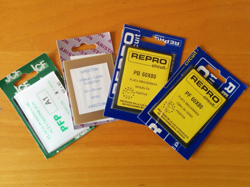
Using photosensitive clads of copper seems easier. You will need:
- A photosensitive clad the size of your design or bigger (between 1 and 2€ for a 60x80 clad)
- Transparency paper (this is costly, 80 cents the sheet of paper)
- A laser or inkjet printer.
- Positive photosensitive developer.
- A (polystyrene) tray.
- Safety glasses, dust mask and gloves.
-
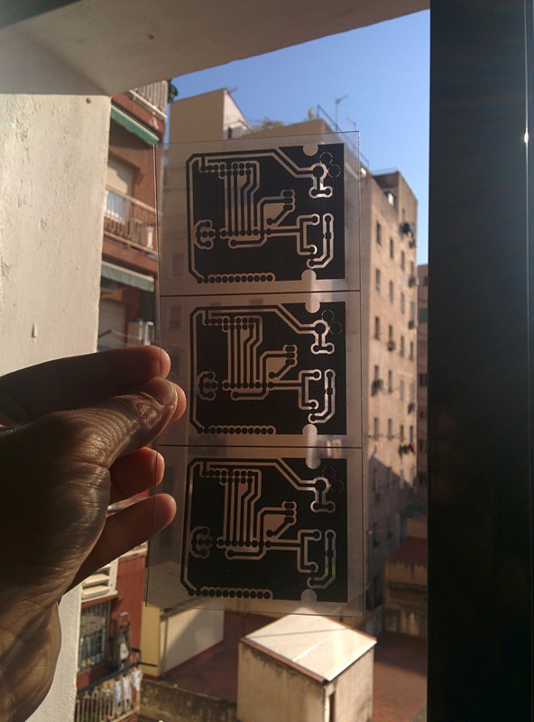
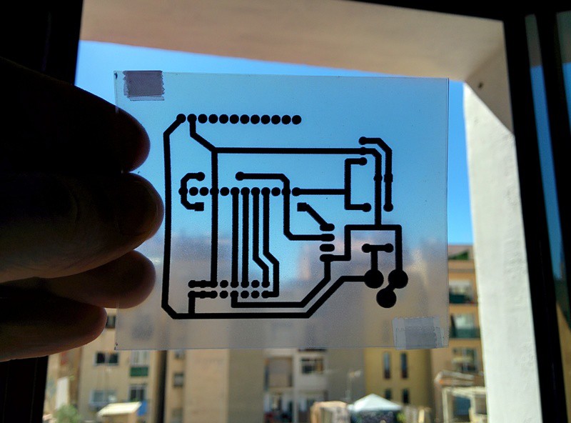
Print several copies (3-4) of your design to a transparency in high quality black and white. To get the circuit image from Eagle I use an Eagle ULP by Niels Springob to export the bottom, pads, vias and holes layers to SVG (get it here). Then I open the file with Inkscape to do the final touches: transform it to B&W, adjust some widths and pads and add a frame around the design. The frame will match the size of the board. I then group it all and make 3 or 4 copies side by side and send it to the printer. I don't have a laser printer but an inkjet printer works just fine.
![image]()
Three in a row, ready to cut and stack (these are version 1.1) -
Cut them by the frame lines and** stack them** one by one using transparent tape to make sure they keep aligned. The goal is to prevent UV beams to pass through the dark parts, so the darker the better.
![image]()
Printed circuit in a transparency with and inkjet printer -
Cut the photosensitive board to the size of the frame you have drawn in step 1. Depending on the wrapping this can be easy or not. I have used two different brands: one has a dark sticker covering the photosensitive side of the board, you can safely cut the board with the sticker on. The other comes wrapped in a black cardboard envelope ad if you want to cut it you have to do it in the dark. Here the goal is, again, to have less copper to etch.
![image]()
Several types and brands of photosensitve copper clads -
Now go to a dark room and prepare a sandwich. My way is a sheet of plywood, the clad of copper with the photosensitive side facing up (peel off the protection sticker first if any!), the stack of transparencies and an acrylic sheet. Everything held in place with a pair of sergeants. Take your time and check twice the orientation of the transparencies. Since they show the bottom layer the printed side should touch the clad.
![image]()
On my second test I wronged the photosensitive side and ended up having a nice silkscreen -
Now it's time for a sun bath. Ten minutes of direct sun works OK for me. Off course you can use those UV boxes but they are really expensive and some people have reported than using a regular fluorescent lamp (daylight range, about 5000K light temperature) works just as fine. Sun stays as the cheapest solution, thou. One advice: make sure the sun beams fall perpendicular to the clad, otherwise you will have some shadow due to the transparencies further from the clad that might prevent the copper in the clearances to be exposed to the acid, potentially creating short-cuts in your circuit. If that happens, like it did to me, you can use a cutter or the Dremel to cut them.
![image]()
A stack of four transparencies already under the sun -
In the meantime, prepare the developer solution. You can try to create yourself the solution at home using Sodium Hydroxide 1% (ten grams of NaOH pellets in a litter of pure water). Caution: Sodium Hydroxide is very caustic, it can burn your skin and you will have a very bad time if it splashes in your eyes. So this is the point when you have to put gloves, dust mask and glasses on. Some say the result quality is very sensitive to the concentration so I went the safe side and bought a bottle of developer ("revelador de placa positiva” in spanish) at the same store where I bought the photosensitive clads (3.80€ to get 3 litters of solution).
-
The 10 minutes countdown is finished and you are back to the dark room with the clad. Now place it in the developer solution and agitate it (gloves on!). In a few seconds the traces will start to show up. Agitate and check every 10 seconds until you see no change in the contrast between the exposed and non exposed zones of the clad, the traces should be clear and well defined. The whole developing process takes about one minute. If you are using thin traces be careful not to let it too long in the developer or they might get damaged.
-
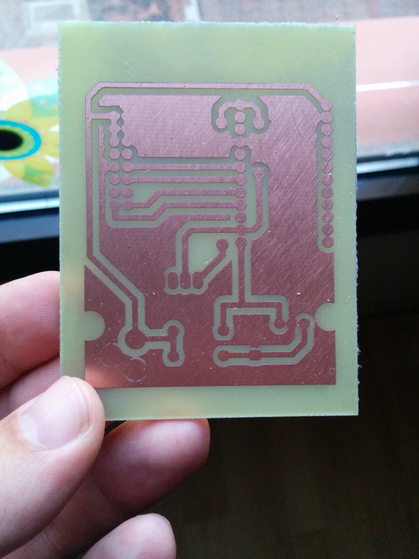
Remove the developer from the clad surface with running water.
![image]()
The photosensitive clad just after developing
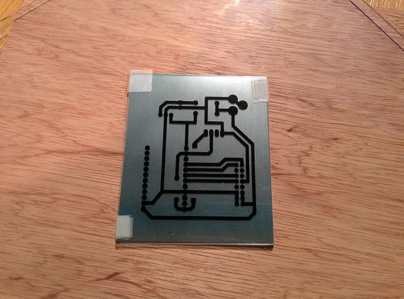
Now you have a ready-to-etch clad. The copper in the zones exposed to the sun beams will be removed by the acid in the next step.
Etching
Here it comes the critical and worrisome step. But it's really easy. You will need:
- Vinegar (acetic acid). I use cleaning vinegar, 7% acidity, 0.70€ the litter at the local supermarket)
- Hydrogen Peroxide. Easy to find at any drugstore, the one I use is 3% peroxide in pure water, 1.20€ 1/2 litter.
- Kitchen salt.
- Acetone, nail polish remover.
- Polystyrene tray. I guess any tray will do as long as the vinegar does not degrade it.
- A brush. I use a teeth brush.
- Plastic tongs to grip the PCB in the solution.
- Again safety glasses, dust mask and gloves.
-
Put your glasses, dust mask and gloves on. OK, this is not Hydrogen Chloride but it is still an acid and the residue is Copper Acetate which is toxic to humans and very toxic to plants, even in low concentrations.
-
Prepare a 50-50 solution of vinegar and hydrogen peroxide in the tray and place the clad in the solution
-
Heating the solution helps a lot. I place the tray with the solution in a bigger tray with hot water that I change every 10-15 minutes. Some people pre-heat the vinegar (alone) in the microwaves before adding the peroxide. I guess you could also use some double boiling technique or maybe a peltier cell bellow the tray to keep the solution warm.
-
Kitchen salt also helps. With the clad in the solution keep pouring salt with a coffee spoon until the fizzing stays by itself.
-
Brush the clad every few minutes to remove the Copper Oxide and Copper Acetate. You will notice that by the end of the process you can actually remove the remaining copper layer by brushing it off.
-
If the fizzing seems to recess, add more salt. If that still doesn't work add more vinegar and Hydrogen Peroxide. I always start with a 50-50 solution but a tend to add more vinegar than peroxide after that. Still trying to find the right ratio.
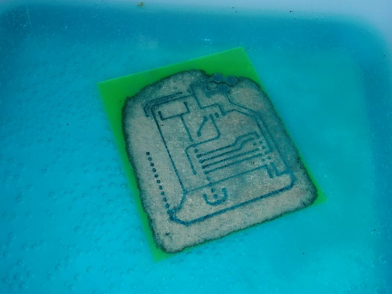
![image]()
The etchant biting the copper -
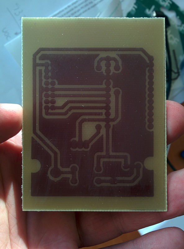
Once all the copper has been removed clean the board with running water and save the solution (see “disposal” below). Then remove the resist with cotton soaked in acetone or a brass sponge.
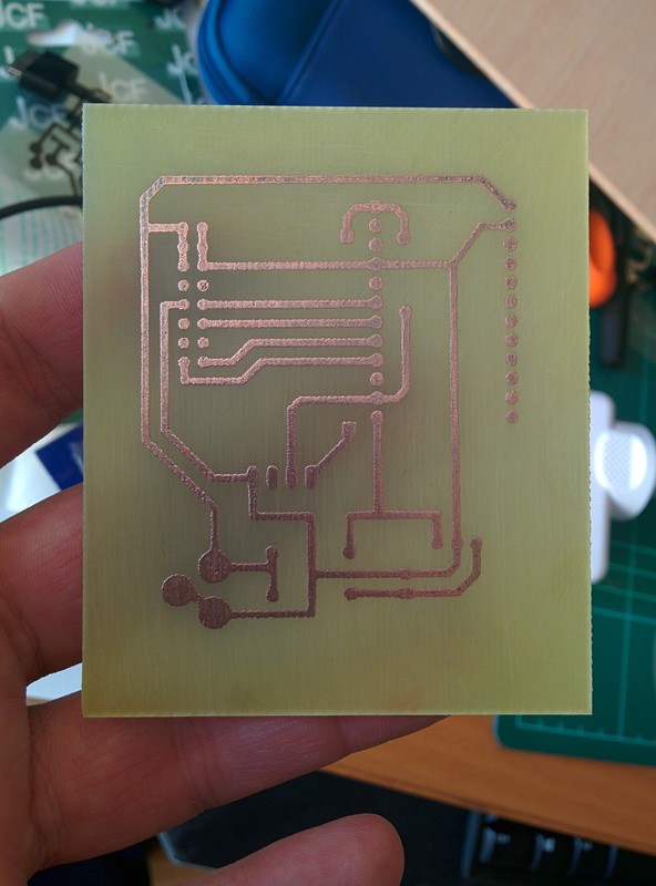
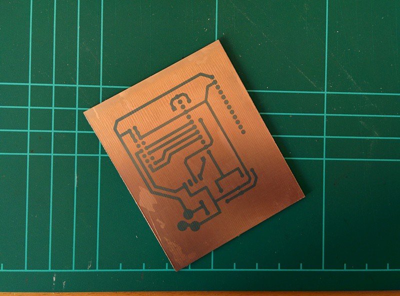
![image]()
Nice copper traces after etching and cleaning
The process is very slow compared to etching with stronger acids but you can easily etch a medium size clad within an hour without complex tooling (bubble machines, heaters,…). The key is to keep it bubbling:
Assembly
Drilling and soldering looked to me like being back to the comfortable zone. But I was wrong. You better have a very steady hand or some tooling aid. A drill press will ease thing a lot. I don't have one so I suffered for what I've named the SDT or Syndrome of the Dancing Tip.
My not-so-good solution is to use the 565 Multipurpose Cutting Kit by Dremel leaving the nut loose to move the drill up and down. It still has some horizontal movement but I can safely drill in the copper pads.
Anyway, what you will need for sure is:
- A drill with tiny bits (get three or four from 0.5 to 1.5 mm)
- Again safety glasses and dust mask.
- Solder iron and lead-free solder
There is not much to say. Maybe some tips:
- Inhaling copper dust is really really bad on the long term. It can produce a wide spectrum of lung diseases and cancer. So always use a mask when drilling copper. Same for soldering fumes. Wash your hands when done.
- If you can, avoid hitting the clad with the drill bit shank (where it gets wider). If you do you will get a nice volcanoe-like hole. Not something to throw your PCB to the trash but certainly ugly.
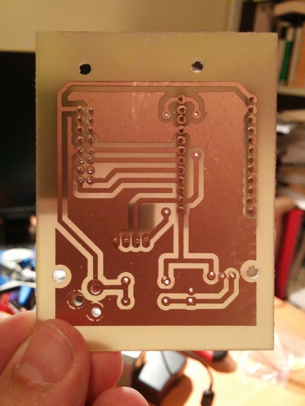
- Test that your components fit in their holes. You will probably have to widen some of them.
![image]()
It took some time to accommodate the headers in their new home... - I have not tested yet, but using Flux (Kontakt SK-10, for instance) on the copper side of the board before soldering should ease the process and flux doubles as protecting coating. You can also clean it with Isopropyl Alcohol before applying flux.
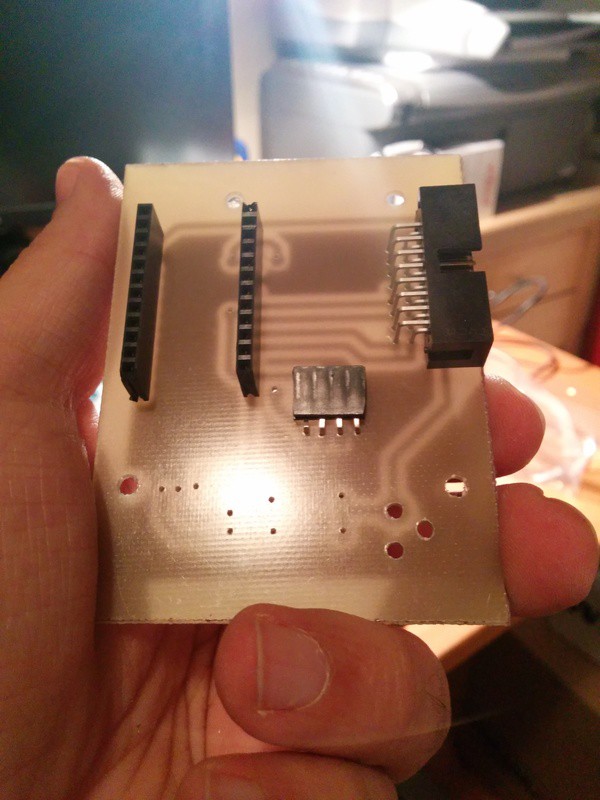
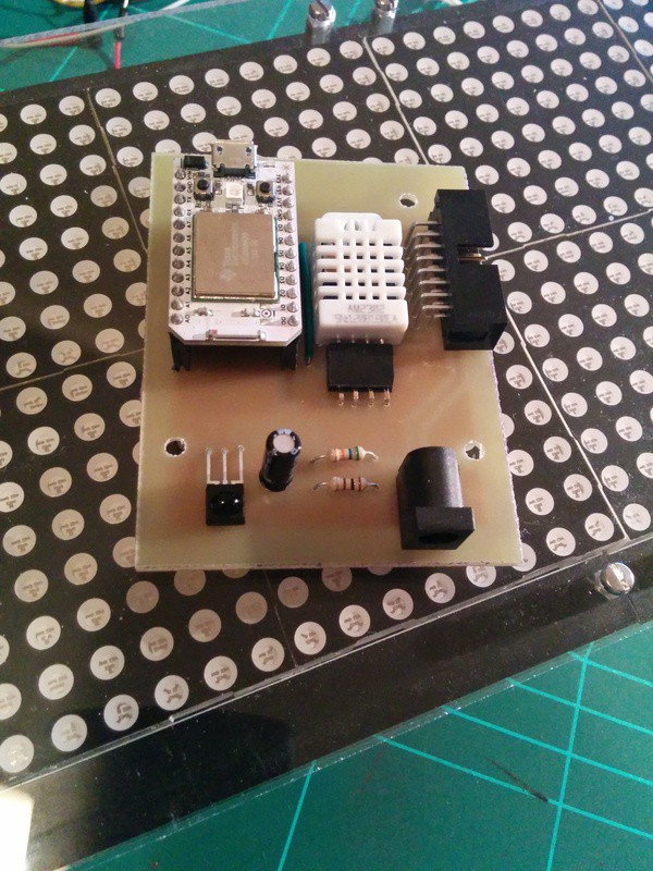
- Have a copy of your schema and board layout at hand. Mind there is no silkscreen and it's always a sinking feeling when you solder your component the other way round.
![image]()
The final result is quite nice
Disposal
Please don't pour it down the drain. Yes, wastewater treatment plants are there but it's also our responsibility. Your first option is reuse. An old solution is yet slower than a fresh one but it can still bit some copper away. Once it's no longer useful to etch you can dispose it in two ways:
-
Using baking soda (sodium bicarbonate). Add baking soda to the solution until it becomes cloudy and turns green. The result (Cupric Carbonate and Sodium Acetate) does not dissolve in water so it's less harmful to the environment. You can then seal it in a plastic container and carry it to the closest disposal unity or place it in the trash.
-
Evaporating the etchant leaving it under the Sun. The result will be greenish crystals of Cupric Acetate which can be safely trash or even better: burn them in a camp fire to get nice green flames!
Whatever method you use manipulate the solution and the results using gloves.
Conclusions
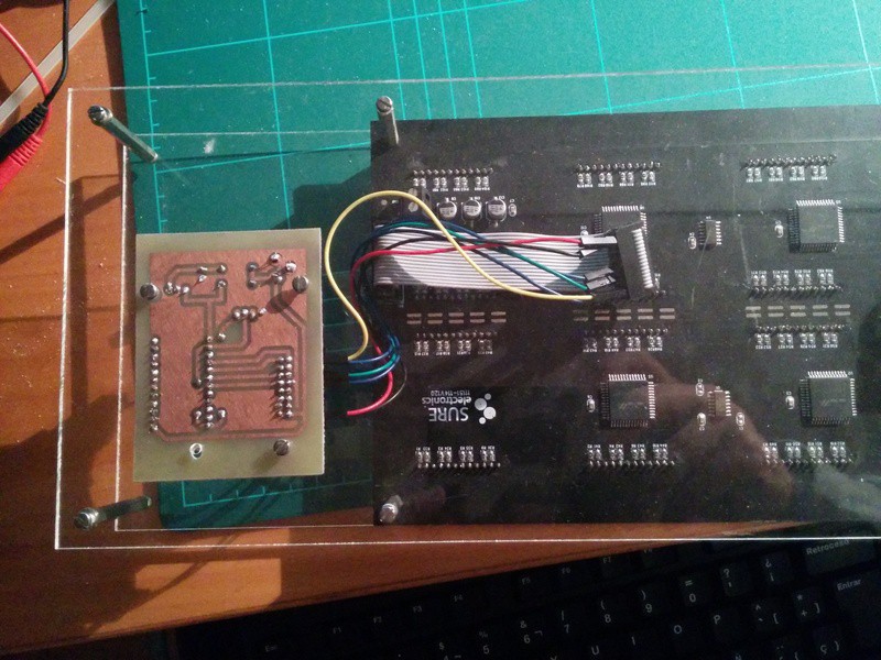
Learning is a never ending work in progress. After the first 3 iterations I discovered a fatal error in the original design: the connector for the led matrix was upside down. The board is still usable with the help of some wires to fix the mistake but a new version is ready for the vinegar tray!
References
I'm adding here some web-references to pages I've checked during these last weeks.
- http://m.wikihow.com/Etch-a-Circuit-Board
- http://www.eham.net/ehamforum/smf/index.php?topic=93977.0
- http://hackaday.com/2012/02/15/etching-pcbs-with-vinegar/
- http://m.instructables.com/id/Sponge-Ferric-Chloride-Method-Etch-Circuit-Bo/
- http://hackaday.com/2008/07/28/how-to-etch-a-single-sided-pcb/
- http://technicaltom.wordpress.com/2013/06/19/a-safer-pcb-etchant-for-young-makers/
- http://quinndunki.com/blondihacks/?p=835
- http://www.stephenhobley.com/blog/2011/03/02/still-messing-with-forces-i-dont-understand-the-formula/
- http://www.opencircuits.com/Chemical_Etchants
- http://www.electricstuff.co.uk/pcbs.html
- http://sfprime.net/pcb-etching/
"PCB etching at home using vinegar" was first posted on 23 April 2014 by Xose Pérez on tinkerman.cat under Learning, Projects, Tutorial and tagged acetic acid, acetone, board layout, developer, dremel, eagle, environment, etching, flux, hydrogen peroxide, isoporpyl alcohol, pcb, photosensitive copper clad, residues, salt, sodium bicarbonate, transparency, vinegar.